
Trace width decides how much current a copper track can carry before it overheats, and how much voltage it wastes on the way. This guide walks through the IPC-2221 method step by step: what each input means, the formula, a worked example, reference tables and the mistakes that cause hot or failing power traces.
Key takeaways
- Four inputs set the width: current, allowed temperature rise, copper thickness and layer type (external or internal).
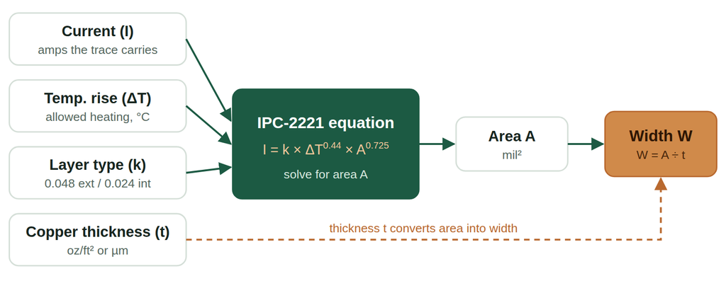
- IPC-2221 gives the current limit as I = k × ΔT^0.44 × A^0.725. Solve it for the copper area A, then divide by copper thickness to get width.
- Width does not grow in a straight line with current. Doubling the current needs about 2.6 times the width.
- Internal traces need about 2.6 times the area of external traces for the same current and temperature rise.
- After the thermal calculation, always check resistance and voltage drop, then add margin.
Why PCB trace width matters
A trace is a thin copper resistor. Current flowing through it produces heat (I²R), and that heat has to leave through the board and the surrounding air. If the trace is too narrow, four problems follow:
- Overheating. The trace temperature climbs above ambient. Standard FR-4 laminate has a glass transition temperature of roughly 130–170 °C, and long-term heat ages the board well before that.
- Voltage drop. A narrow trace has higher resistance, so the load sees less voltage. This matters for low-voltage rails and battery products.
- Reliability. Hot spots stress solder joints, vias and nearby components.
- Wasted energy. Resistive loss turns directly into heat inside your enclosure.
The opposite mistake, making every trace wide, wastes routing space and can make a dense board impossible to route. The goal is the narrowest trace that stays safely within your temperature and voltage-drop limits.
What determines the trace width
Four design inputs go into the IPC-2221 equation, which returns the copper cross-section area. Dividing that area by the copper thickness gives the width.
Current (I)
The continuous current the trace must carry, in amps. Use the RMS or steady value for heating, and add a margin of 20–30% for component tolerance and future changes.
Temperature rise (ΔT)
How many degrees the trace may heat above the surrounding temperature. A 10 °C rise is a conservative default. Rugged designs often accept 20–30 °C. The final trace temperature is ambient plus the rise, so a 40 °C enclosure with a 20 °C rise runs the copper at about 60 °C.
Copper thickness (t)
Copper weight is quoted in ounces per square foot. One ounce spreads to a layer about 35 µm (1.378 mil) thick. Thicker copper carries the same current in a narrower trace.
Layer type (k)
External traces lose heat to the air, so IPC-2221 uses k = 0.048. Internal traces are buried in laminate, so it uses k = 0.024.
The IPC-2221 trace width formula
IPC-2221 is the generic standard for printed board design. Its current-carrying equation was fitted to test data and is written in mils and amps:
I = k × ΔT^0.44 × A^0.725
To find the width, rearrange the equation for area and then divide by the copper thickness:
A = ( I ÷ ( k × ΔT^0.44 ) ) ^ (1 ÷ 0.725)
W = A ÷ t
| Symbol | Meaning | Unit |
|---|---|---|
| I | Current the trace carries | A |
| ΔT | Allowed temperature rise above ambient | °C |
| k | Layer constant: 0.048 external, 0.024 internal | none |
| A | Copper cross-section area (width × thickness) | mil² |
| t | Copper thickness, 1.378 mil per oz | mil |
| W | Trace width | mil (or mm) |
Multiply mil by 0.0254 to get millimetres.
Why internal layers are different
An external trace sheds heat into the air above it. An internal trace is sandwiched between laminate layers, which conduct heat poorly, so it runs hotter for the same current.
Because k is half as large for internal layers, the internal area is 2^(1/0.725), or about 2.6 times the external area, at the same current and temperature rise. Later research in IPC-2152 found that internal traces run cooler than IPC-2221 assumes, so the internal result is on the safe side.
Copper thickness and copper weight
Fabricators specify copper by weight. The thickness values below are the ones to use in the formula.
| Copper weight | Thickness (µm) | Thickness (mil) | Typical use |
|---|---|---|---|
| 0.5 oz | 17.5 | 0.689 | Fine-pitch signal layers, many inner layers |
| 1 oz | 35 | 1.378 | Standard outer layers, general power |
| 2 oz | 70 | 2.756 | Higher-current power boards |
| 3 oz | 105 | 4.134 | Heavy-copper power boards |
Thicker copper makes etching of fine traces harder, so check the minimum trace and space your manufacturer offers for the copper weight you choose.
How to calculate PCB trace width step by step
- Set the current. Use the continuous current and add 20–30% margin.
- Choose the temperature rise. Start at 10 °C unless you have thermal margin to spare.
- Pick the copper weight. Use what your fabricator offers on that layer, usually 1 oz outside.
- Select the layer type. Use k = 0.048 for external, k = 0.024 for internal.
- Solve for area. A = (I ÷ (k × ΔT^0.44)) ^ (1/0.725), in mil².
- Convert area to width. W = A ÷ t, with t in mil. Multiply by 0.0254 for millimetres.
- Check the electrical drop. Resistance is R = ρ × L ÷ (W × t). Copper has ρ = 1.724 × 10⁻⁸ Ω·m at 20 °C and rises about 0.393% per °C. Multiply R by the current to get the voltage drop, and by I² to get power loss.
- Add margin and verify. Round up to a practical width. For critical or high-current nets, cross-check with IPC-2152, a thermal simulation or a prototype test.
Worked example: 3 A on a 1 oz outer layer
Suppose a motor driver rail carries 3 A. The board uses 1 oz copper, the trace is on an external layer, you allow a 10 °C rise, and the trace is 100 mm long in a 25 °C environment.
- Layer constant: k = 0.048 (external).
- Temperature term: ΔT^0.44 = 10^0.44 = 2.754.
- Denominator: k × ΔT^0.44 = 0.048 × 2.754 = 0.1322.
- Ratio: I ÷ 0.1322 = 3 ÷ 0.1322 = 22.69.
- Area: A = 22.69^(1/0.725) = 74.2 mil².
- Width: W = 74.2 ÷ 1.378 = 53.8 mil, or 1.37 mm.
Electrical check at 35 °C trace temperature. Resistivity at 35 °C is 1.826 × 10⁻⁸ Ω·m. For 100 mm of 1.37 mm by 35 µm copper the resistance is about 38.2 mΩ. At 3 A that is a drop of roughly 114 mV and a power loss of about 343 mW. That is acceptable on a 12 V rail, but would deserve a second look on a 1.8 V rail.
Same trace on an internal layer. With k = 0.024 the ratio becomes 45.38, the area 192.9 mil² and the width 140.0 mil (3.56 mm), about 2.6 times wider. If routing space is tight, an external layer or thicker copper is the better choice.
Quick reference table
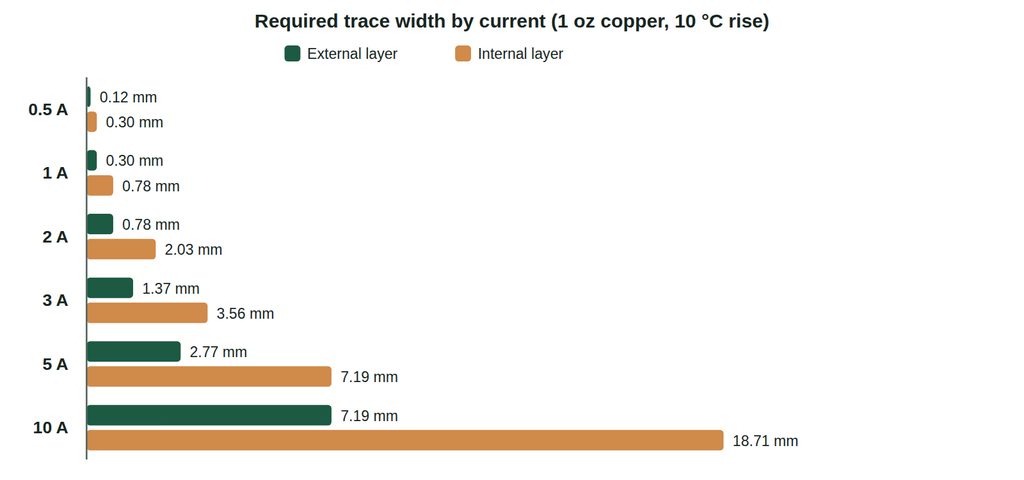
These widths use a 10 °C temperature rise and the IPC-2221 equation. Values are the minimum for heating only, before margin.
| Current | External, 1 oz | Internal, 1 oz | External, 2 oz |
|---|---|---|---|
| 0.5 A | 0.12 mm (4.5 mil) | 0.30 mm (11.8 mil) | 0.06 mm (2.3 mil) |
| 1 A | 0.30 mm (11.8 mil) | 0.78 mm (30.8 mil) | 0.15 mm (5.9 mil) |
| 2 A | 0.78 mm (30.8 mil) | 2.03 mm (80.0 mil) | 0.39 mm (15.4 mil) |
| 3 A | 1.37 mm (53.8 mil) | 3.56 mm (140.0 mil) | 0.68 mm (26.9 mil) |
| 5 A | 2.77 mm (108.9 mil) | 7.19 mm (283.2 mil) | 1.38 mm (54.4 mil) |
| 10 A | 7.19 mm (283.2 mil) | 18.71 mm (736.8 mil) | 3.60 mm (141.6 mil) |
Notice how quickly the widths grow at higher current. Above roughly 5–10 A, a copper pour, thicker copper or a busbar is usually more practical than a single trace.
How each change affects trace width
The exponents in the equation give fixed multipliers. They are handy for quick what-if checks while routing.
- Doubling the current makes the trace about 2.60 times wider.
- Doubling the copper weight makes the trace about 0.50 times as wide (half).
- Moving from an external to an internal layer makes the trace about 2.60 times wider.
- Raising the temperature rise from 10 °C to 20 °C makes the trace about 0.66 times as wide.
The table shows how the 3 A example changes with temperature rise and copper weight on an external layer.
| Temperature rise | 0.5 oz | 1 oz | 2 oz |
|---|---|---|---|
| 10 °C | 2.73 mm | 1.37 mm | 0.68 mm |
| 20 °C | 1.80 mm | 0.90 mm | 0.45 mm |
| 30 °C | 1.40 mm | 0.70 mm | 0.35 mm |
Design tips and common mistakes
- Calculate for the narrowest point. A long wide trace with one narrow neck is only as strong as the neck. Keep neck-downs at pads as short as possible.
- Do not forget voltage drop. A trace can pass the thermal check and still lose too much voltage over a long run.
- Use copper pours for heavy current. Planes and pours spread heat and have very low resistance.
- Mind vias. A via carries far less current than a wide trace. Use several vias in parallel when a power net changes layers.
- Allow for neighbouring heat sources. Regulators, MOSFETs and resistors warm nearby copper, and the real rise can exceed the calculated one.
- Treat high voltage separately. Trace width does not set creepage and clearance. Spacing between conductors follows its own rules in IPC-2221.
- Check manufacturing limits. Many fabricators offer a minimum trace of roughly 0.1–0.15 mm on standard processes. Confirm yours before finalising.
Limits of the IPC-2221 method
IPC-2221 is based on older chart data and works best for roughly 10–100 °C rise, 0.5–3 oz copper and currents up to about 35 A. It assumes steady DC current in a straight, isolated trace in still air. It does not model airflow, nearby copper planes, board thickness, short pulses or high-frequency skin effect. IPC-2152 covers many of these and is the better reference for demanding designs.
Frequently asked questions
What is the formula for PCB trace width?
Use the IPC-2221 equation I = k × ΔT^0.44 × A^0.725 to find the copper area A for a given current I and temperature rise ΔT, with k = 0.048 for external and 0.024 for internal layers. Then divide A by the copper thickness to get the width.
How wide should a trace be for 1 A, 2 A and 3 A?
On a 1 oz external layer with a 10 °C rise, IPC-2221 gives about 0.30 mm for 1 A, 0.78 mm for 2 A and 1.37 mm for 3 A. Add margin and check the voltage drop before settling on a value.
Does trace length affect the required width?
Not for the heating calculation. Length does set the resistance, voltage drop and power loss, so long traces on low-voltage rails may need to be wider than the thermal result.
Why do internal traces need to be wider than external ones?
Internal traces lose heat only through the laminate, while external traces can also lose heat to the air. IPC-2221 reflects this with k = 0.024 instead of 0.048, which means about 2.6 times more copper area for the same current.
What temperature rise should I use?
10 °C is a common, conservative choice. 20–30 °C can be acceptable when the product has thermal margin. Use a smaller rise for precision circuits, hot environments or long-life products.
Should I use IPC-2221 or IPC-2152?
IPC-2221 is simple and conservative, which makes it good for quick sizing. IPC-2152 is newer and accounts for board thickness, nearby copper planes and airflow, so it is better for critical or high-current designs.
Can I use a thinner trace if I use thicker copper?
Yes. For a fixed current the required copper area stays the same, so doubling the copper thickness halves the width. Check that your manufacturer can etch the finer features at that copper weight.
How do I size a trace for pulsed current?
Heating follows the RMS current, so use that for the thermal calculation. Very short pulses benefit from the thermal mass of the copper, but you should verify peak-current limits separately and test the design.
Conclusion
Calculating PCB trace width comes down to four inputs and one equation: choose the current, temperature rise, copper weight and layer, solve for area, and divide by thickness. Then check voltage drop, add margin and verify critical nets. With the tables above you can size power traces quickly and with confidence.