
Complete Guide to SMT PCB Assembly Manufacturing
Surface Mount Technology (SMT) is one of the most widely used methods for manufacturing modern electronic products. SMT allows electronic components such as resistors, capacitors, diodes, transistors, ICs, microcontrollers, memory devices and connectors to be mounted directly onto the surface of a printed circuit board (PCB).
A modern SMT PCB assembly line combines automated machines, controlled process parameters, inspection systems and electrical testing to produce reliable electronic assemblies.
The complete SMT PCB assembly process can be represented as:
Component Receiving → Component Kitting → Solder Paste Printing → SPI Inspection → Component Pick and Place → Reflow Soldering → AOI Inspection → Rework → Conformal Coating → Functional Testing → Final Inspection → Traceability → Packing
Every process stage has a specific purpose. Controlling each stage is essential because a defect introduced during an earlier process can become more difficult and expensive to correct at a later stage.
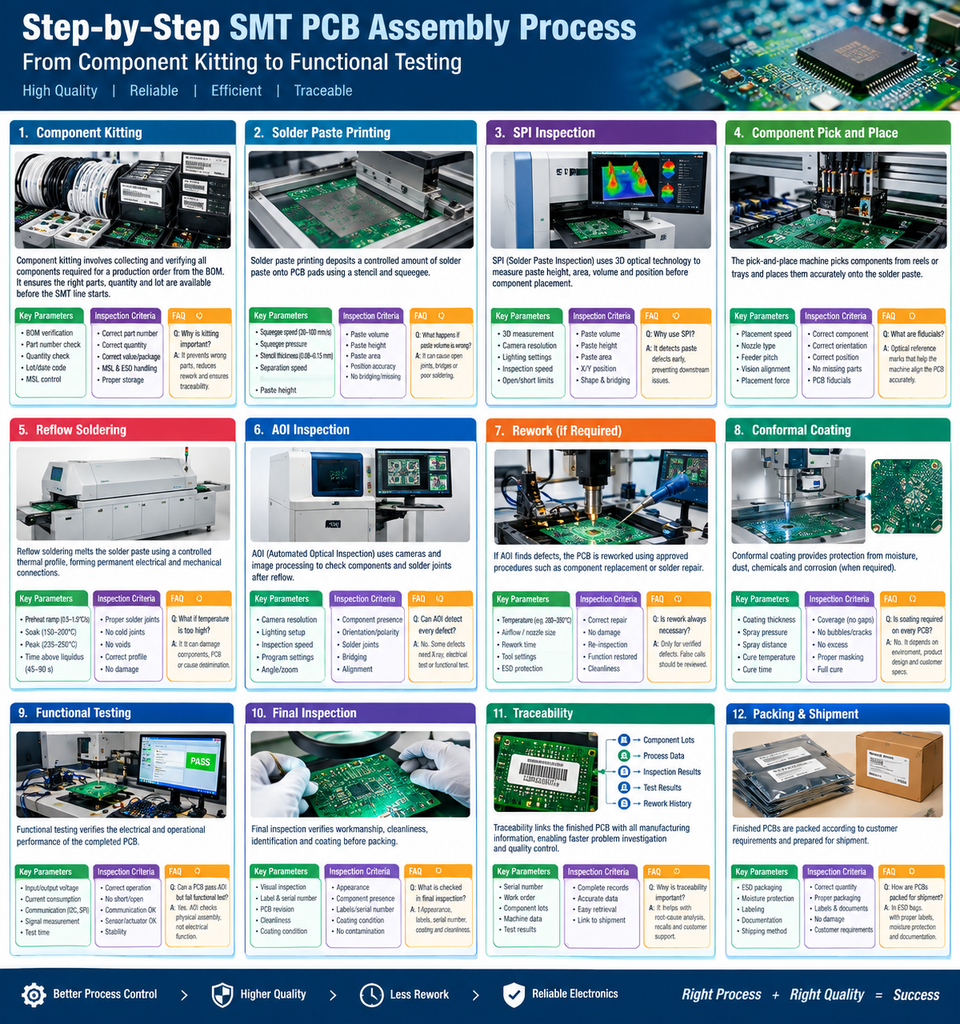
SMT PCB Assembly Process Flow
PCB and Component Receiving
↓
Component Kitting
↓
Solder Paste Printing
↓
SPI Inspection
↓
Component Pick and Place
↓
Reflow Soldering
↓
AOI Inspection
↓
Rework / Touch-Up if Required
↓
Conformal Coating if Required
↓
Functional Testing
↓
Final Inspection
↓
Traceability
↓
Packing and Shipment
1. Component Receiving and Component Kitting
Component kitting is the material preparation stage of SMT PCB assembly.
Before production starts, all components required for a particular PCB assembly are collected according to the approved Bill of Materials (BOM).
Typical SMT production materials include:
- Resistors
- Capacitors
- Diodes
- Transistors
- ICs
- Microcontrollers
- Memory devices
- Voltage regulators
- LEDs
- Sensors
- Connectors
The component stores or material-control team verifies the required components and prepares them for the SMT production line.
Component Kitting Process
Production Work Order
↓
BOM Verification
↓
Part Number Verification
↓
Manufacturer Verification
↓
Quantity Verification
↓
Lot / Date Code Verification
↓
MSL Verification
↓
Component Storage Verification
↓
Feeder Preparation
↓
SMT Production
Component Kitting Inspection Criteria
| Inspection Item | Requirement |
|---|---|
| Part Number | Must match approved BOM |
| Component Value | Must match BOM |
| Package | Must match PCB footprint |
| Manufacturer | Approved manufacturer where applicable |
| Quantity | Sufficient quantity |
| Lot Number | Record for traceability |
| Date Code | Verify according to requirements |
| MSL | Verify moisture sensitivity |
| Polarity | Verify polarity-sensitive components |
| ESD | Follow ESD handling requirements |
| Component Condition | No visible damage |
Important Kitting Controls
Wrong component selection can create serious problems.
For example, two components may have similar physical packages but completely different electrical characteristics.
Therefore, component identification should consider:
- Manufacturer part number
- Component value
- Package
- Datasheet
- Barcode
- Lot number
- Date code
- BOM revision
Component Kitting Machine / Tools
Typical equipment includes:
- Barcode scanner
- Component storage system
- Dry cabinet
- ESD workstation
- Reel racks
- Component counting machine
- SMT feeders
Component Kitting FAQ
Why is component kitting important?
Component kitting ensures that the correct components are available before production begins. It reduces wrong-component loading and improves manufacturing traceability.
What happens if the wrong component is loaded?
The PCB may be assembled incorrectly even though the SMT machine operates normally. The error may be detected by AOI or functional testing, but preventing the error during kitting is much better.
What is MSL in component handling?
MSL means Moisture Sensitivity Level. It defines the moisture sensitivity of certain semiconductor packages and determines how they should be stored and handled before reflow.
Why is component traceability important?
Traceability allows the manufacturer to identify component lots used on a particular PCB, which helps during failure analysis and quality investigations.
2. Solder Paste Printing
Solder paste printing is the first major PCB assembly operation.
The purpose of this process is to deposit a controlled quantity of solder paste onto the PCB solder pads.
A metal stencil contains apertures corresponding to the PCB solder pads.
Solder paste is placed on the stencil and a squeegee moves across the stencil.
The paste passes through the stencil apertures and is transferred onto the PCB pads.
Solder Paste Printing Process
PCB Loading
↓
Stencil Alignment
↓
Solder Paste Application
↓
Squeegee Movement
↓
Paste Transfer
↓
Stencil Separation
↓
Printed PCB
Main Solder Paste Printer Components
A typical solder paste printer contains:
- PCB conveyor
- PCB support system
- Stencil
- Stencil frame
- Squeegee
- Solder paste
- Vision camera
- Alignment system
- Stencil cleaning system
- Control software
Solder Paste Printing Parameters
| Parameter | Typical Starting Consideration |
|---|---|
| Squeegee Speed | Approximately 20–100 mm/s |
| Squeegee Pressure | Machine/stencil/paste dependent |
| Stencil Thickness | Often around 0.08–0.15 mm depending on design |
| Separation Speed | Controlled according to stencil/paste |
| PCB Support | Required for stable printing |
| Paste Condition | Must meet manufacturer requirements |
| Stencil Cleaning | Based on process requirements |
| Print Alignment | Must be controlled |
These values are general starting points. Actual production parameters should be established using the solder paste manufacturer’s recommendations, stencil design and PCB requirements.
Important Printing Factors
Solder paste printing quality depends on:
- Stencil thickness
- Aperture design
- Solder paste condition
- Squeegee speed
- Squeegee pressure
- PCB support
- Stencil cleanliness
- PCB-to-stencil alignment
- Paste handling
- Stencil separation
Common Printing Defects
| Defect | Possible Cause |
|---|---|
| Insufficient Paste | Blocked aperture |
| Excess Paste | Excessive paste transfer |
| Paste Bridging | Excess paste / aperture issue |
| Paste Offset | Alignment problem |
| Missing Paste | Blocked aperture |
| Uneven Deposit | PCB support problem |
| Smearing | Printing/separation issue |
| Poor Release | Stencil/paste condition |
Solder Paste Printing FAQ
What is solder paste printing?
It is the process of depositing solder paste onto PCB pads using a stencil.
Why is stencil thickness important?
Stencil thickness affects the quantity of solder paste deposited onto the PCB pads.
What happens if too much solder paste is printed?
Excess solder paste can increase the possibility of solder bridging and other solder-joint defects.
What happens if too little solder paste is printed?
Insufficient solder paste can result in weak solder joints, insufficient solder volume or open connections.
Why is PCB support required during printing?
PCB support prevents the board from flexing and helps maintain accurate stencil-to-PCB contact.
3. SPI – Solder Paste Inspection
SPI stands for Solder Paste Inspection.
SPI is performed immediately after solder paste printing and before component placement.
The SPI machine uses optical inspection technology, commonly including 3D measurement, to inspect the solder paste deposits.
The system measures parameters such as:
- Paste height
- Paste area
- Paste volume
- X position
- Y position
- Paste shape
SPI Inspection Flow
Solder Paste Printing
↓
SPI Inspection
↓
3D Image Capture
↓
Paste Measurement
↓
Compare With Limits
↓
PASS / FAIL
SPI Inspection Criteria
| Parameter | Inspection Purpose |
|---|---|
| Paste Volume | Verify solder quantity |
| Paste Height | Verify deposit height |
| Paste Area | Verify coverage |
| X Position | Verify alignment |
| Y Position | Verify alignment |
| Paste Shape | Detect abnormal deposit |
| Missing Paste | Detect absence |
| Bridging | Detect possible shorting condition |
Why SPI Is Important
SPI provides early process feedback.
Without SPI:
Printing → Pick and Place → Reflow → AOI → Defect
With SPI:
Printing → SPI → Detect Defect → Correct Process → Continue Production
This makes SPI an important process-control tool.
SPI Machine Parameters
Typical controlled parameters include:
- Camera resolution
- Lighting
- Inspection speed
- 3D measurement settings
- Inspection thresholds
- Reference data
- Board alignment
- Inspection window
The actual settings depend on the SPI equipment and PCB design.
SPI FAQ
What does SPI stand for?
SPI stands for Solder Paste Inspection.
What is the main purpose of SPI?
The main purpose is to verify whether solder paste has been correctly deposited before component placement.
What does SPI measure?
SPI commonly measures solder paste height, area, volume and position.
Why is SPI performed before pick and place?
Because solder paste defects are easier to correct before components are mounted.
Can SPI inspect component placement?
No. SPI primarily inspects solder paste. Component placement is normally inspected using machine vision and AOI.
4. Component Pick and Place
After SPI inspection, components are mounted onto the PCB using an automated pick-and-place machine.
The machine receives components from reels, trays or other feeders.
A pickup nozzle collects the component, the vision system identifies its position and orientation, and the machine places it accurately onto the solder paste deposit.
Pick and Place Process
Component Reel / Tray
↓
Feeder
↓
Pickup Nozzle
↓
Component Pickup
↓
Vision Recognition
↓
Orientation Correction
↓
PCB Fiducial Recognition
↓
Component Placement
Main Pick-and-Place Parameters
| Parameter | Purpose |
|---|---|
| Placement Speed | Production throughput |
| Pickup Position | Reliable component pickup |
| Placement Position | Accurate location |
| Nozzle Type | Matches package |
| Feeder Pitch | Component presentation |
| Component Rotation | Correct orientation |
| Vision Settings | Component recognition |
| Fiducials | PCB alignment |
| Placement Force | Component seating |
PCB Fiducials
Fiducials are optical reference marks placed on the PCB.
They help the SMT machine determine the exact PCB position.
Typical arrangement:
Global Fiducials → PCB Alignment → Local Fiducials → Fine Component Placement
Pick-and-Place Inspection Points
The manufacturing engineer should verify:
- Correct feeder
- Correct part number
- Correct package
- Correct nozzle
- Correct orientation
- Correct polarity
- Correct placement location
- Correct rotation
- Correct placement program
- Correct PCB revision
Pick-and-Place FAQ
What does a pick-and-place machine do?
It automatically picks components from feeders or trays and places them onto the PCB.
Why are feeders important?
Feeders present components to the machine in a controlled position so that the pickup nozzle can reliably collect them.
What are fiducials?
Fiducials are reference marks used by the vision system to accurately determine PCB position.
What causes component placement errors?
Possible causes include incorrect program data, feeder problems, nozzle problems, vision errors, component pickup problems or PCB alignment issues.
Why is component orientation important?
Polarity-sensitive components such as diodes, LEDs and ICs must be mounted in the correct orientation for the circuit to operate correctly.
5. Reflow Soldering
Reflow soldering is the process used to melt the solder paste and create permanent electrical and mechanical connections.
The PCB containing the placed components travels through a controlled-temperature reflow oven.
The process normally consists of:
Preheat → Soak → Reflow → Cooling
Reflow Process
PCB With Components
↓
Preheat
↓
Soak
↓
Reflow / Peak
↓
Cooling
↓
Solid Solder Joints
Reflow Thermal Parameters
| Parameter | Example Range / Consideration |
|---|---|
| Preheat Ramp | Approximately 0.5–1.5°C/s |
| Soak Region | Approximately 150–200°C depending on process |
| SAC Liquidus | Around 217°C |
| Time Above Liquidus | Often around 45–90 seconds |
| Peak Temperature | Commonly around 235–250°C depending on paste |
| Cooling Rate | Controlled according to process |
Actual values must follow the solder paste manufacturer’s recommendations and component temperature limits.
Reflow Oven Zones
A typical reflow oven may contain:
- Preheat zones
- Soak zones
- Reflow zones
- Peak-temperature region
- Cooling zones
The number of zones depends on the oven.
Why Reflow Profile Is Important
If temperature is too low:
- Poor solder melting
- Poor wetting
- Cold solder joints
If temperature is too high:
- Component damage
- PCB damage
- Excessive thermal stress
If heating is too fast:
- Thermal shock
- Component stress
If cooling is too fast:
- Mechanical stress
- Possible solder-joint reliability concerns
Reflow Profile Verification
A thermal profiler can be used to measure the actual PCB temperature profile.
Thermocouples may be attached to:
- Large components
- Small components
- PCB centre
- PCB edge
- Sensitive components
- High thermal-mass areas
Reflow FAQ
What is reflow soldering?
Reflow soldering heats solder paste until it melts and forms solder joints between components and PCB pads.
Why is a reflow profile required?
The profile ensures that the PCB reaches the required temperatures for proper soldering without exceeding component or PCB thermal limits.
What happens if the peak temperature is too high?
Components or the PCB can be damaged, and excessive thermal stress may reduce reliability.
What is time above liquidus?
It is the time during which the solder is above its liquidus temperature and remains molten.
How is a reflow profile measured?
A thermal profiler with thermocouples is commonly used to record PCB temperature as it passes through the oven.
6. AOI – Automated Optical Inspection
AOI stands for Automated Optical Inspection.
AOI is normally performed after reflow soldering.
The AOI machine uses cameras, controlled lighting and image-processing software to inspect the PCB assembly.
AOI Inspection Flow
Reflowed PCB
↓
Image Capture
↓
Component Recognition
↓
Position Analysis
↓
Polarity Analysis
↓
Solder Joint Analysis
↓
PASS / FAIL
↓
Operator Verification
AOI Inspection Criteria
| Inspection | What Is Checked |
|---|---|
| Component Presence | Component exists |
| Component Identity | Correct component |
| Orientation | Correct rotation |
| Polarity | Correct direction |
| Position | Within tolerance |
| Solder Joint | Acceptable appearance |
| Bridging | No unwanted connection |
| Alignment | Correct placement |
| Missing Solder | Adequate solder connection |
| Excess Solder | No excessive solder |
Common AOI Defects
- Missing component
- Wrong component
- Component shift
- Component rotation
- Polarity error
- Solder bridge
- Insufficient solder
- Excess solder
- Lifted lead
- Alignment problem
AOI False Calls
AOI can sometimes identify an acceptable condition as a potential defect.
Possible causes include:
- Component reflection
- Solder reflection
- PCB color
- Lighting
- Component appearance variation
- Incorrect inspection limits
Therefore, suspicious AOI results should be reviewed by trained personnel.
AOI FAQ
What does AOI stand for?
AOI stands for Automated Optical Inspection.
What does AOI inspect?
AOI commonly inspects component presence, position, orientation, polarity and visible solder-joint conditions.
Can AOI detect every defect?
No. Some electrical defects and hidden solder-joint defects require other inspection or testing methods.
Why is AOI performed after reflow?
After reflow, components and solder joints have reached their final assembled condition, allowing visual inspection of the completed SMT assembly.
What is an AOI false call?
A false call occurs when AOI identifies a possible defect that is actually acceptable after human verification.
7. SMT Rework and Touch-Up
If AOI identifies a genuine manufacturing defect, the PCB may be transferred to an approved rework station.
Typical rework activities include:
- Component replacement
- Solder bridge removal
- Solder touch-up
- Component alignment correction
- Missing component installation
- Solder-joint repair
Rework Flow
AOI Failure
↓
Operator Verification
↓
True Defect?
↓
YES → Rework
↓
Re-inspection
↓
PASS
Rework Parameters
Depending on the operation, controlled parameters can include:
- Soldering temperature
- Hot-air temperature
- Airflow
- Nozzle size
- Heating time
- Rework time
- Tool settings
- ESD protection
The correct parameters depend on the component, PCB design and approved rework procedure.
Rework Inspection Criteria
After rework, verify:
- Correct component
- Correct orientation
- No component damage
- Good solder joint
- No solder bridge
- No PCB damage
- No lifted pad
- Correct functionality
- Reinspection completed
Rework FAQ
Is rework always required when AOI fails?
No. The AOI result should first be verified. Some AOI failures are false calls.
Why should rework be controlled?
Improper rework can damage components, PCB pads, tracks or solder joints.
What should happen after rework?
The PCB should be reinspected and, where required, functionally tested.
Can every SMT component be reworked?
Many components can be reworked, but the method depends on package type, PCB design, component sensitivity and approved manufacturing procedures.
8. Conformal Coating
Conformal coating is a protective layer applied to the PCB when environmental protection is required.
It can protect the PCB against:
- Moisture
- Humidity
- Dust
- Contamination
- Corrosion
- Condensation
- Certain chemicals
Conformal coating is not required for every PCB. The requirement depends on the product design and environmental requirements.
Conformal Coating Process
Clean PCB
↓
Inspection
↓
Masking
↓
Coating Application
↓
Coverage Inspection
↓
Curing
↓
Final Inspection
Common Coating Types
- Acrylic
- Silicone
- Polyurethane
- Epoxy
- Specialized coatings
Each material has different characteristics.
Areas Requiring Masking
Depending on the product design, masking may be required for:
- Connectors
- Test points
- Switches
- Relays
- Sensors
- Adjustment controls
- Mechanical interfaces
- Certain heat-transfer surfaces
- Certain RF interfaces
Conformal Coating Parameters
| Parameter | Controlled Factor |
|---|---|
| Coating Thickness | Required protection |
| Spray Pressure | Application consistency |
| Spray Distance | Coverage |
| Spray Speed | Uniformity |
| Material Viscosity | Flow |
| Cure Temperature | Cure quality |
| Cure Time | Complete curing |
| Masking | Prevent unwanted coating |
Actual values should be based on the coating manufacturer’s technical documentation and product specification.
Conformal Coating Inspection Criteria
Check for:
- Missing coating
- Excess coating
- Bubbles
- Cracks
- Peeling
- Uneven coating
- Contamination
- Coating on prohibited areas
- Incomplete curing
Conformal Coating FAQ
What is conformal coating?
It is a protective coating applied to the surface of a PCB to improve environmental protection.
Is conformal coating required on every PCB?
No. It depends on the product application and environmental requirements.
Why is masking required?
Masking prevents coating from covering areas where coating is not permitted.
What happens if coating is too thick?
Excessive coating can affect curing, thermal performance, reworkability and certain component or connector functions.
How can coating coverage be inspected?
Depending on the coating system, visual inspection, UV inspection or thickness-related inspection methods may be used.
9. Functional Testing
Functional testing verifies whether the completed PCB actually performs its intended electrical and operational functions.
A PCB can pass visual inspection and still fail functional testing.
For example:
AOI PASS
↓
PCB Looks Correct
↓
Power Applied
↓
Functional Test
↓
PASS / FAIL
Functional Test Parameters
Depending on the product, the test may include:
- Input voltage
- Output voltage
- Current consumption
- Analog signals
- Digital signals
- Communication
- Sensor operation
- Relay operation
- Motor control
- Display operation
- LED operation
- Ethernet
- CAN
- RS-485
- UART
- SPI
- I²C
- USB
- Wireless interfaces
Functional Test Equipment
A test setup may use:
- Test fixture
- Digital multimeter
- Oscilloscope
- DC power supply
- Electronic load
- Function generator
- Communication analyzer
- Programmer
- Debugger
- Automated test software
- Custom test hardware
Functional Test Process
Completed PCB
↓
Test Fixture
↓
Power ON
↓
Firmware / Test Program
↓
Input Signals
↓
Output Measurement
↓
Communication Test
↓
Functional Verification
↓
PASS / FAIL
Functional Testing FAQ
What is functional testing?
Functional testing verifies whether the PCB performs its intended electrical and operational functions.
Why can a PCB pass AOI but fail functional testing?
AOI mainly checks physical assembly characteristics. Electrical, firmware, programming or circuit-level problems may not be visible.
What equipment is used for functional testing?
Equipment can include power supplies, multimeters, oscilloscopes, electronic loads, communication analyzers and automated test fixtures.
Is functional testing required for every PCB?
The required level of testing depends on the product, customer requirements and risk level.
What is an automated functional test?
An automated functional test uses a test fixture and software to automatically apply inputs, measure outputs and determine PASS or FAIL.
10. Final Inspection
Final inspection is performed after manufacturing and testing are completed.
The purpose is to confirm that the finished PCB meets the required workmanship and product requirements before shipment.
Final Inspection Criteria
Check:
- PCB appearance
- Component presence
- Component orientation
- Solder workmanship
- Coating condition
- Labels
- Serial number
- PCB revision
- Cleanliness
- Test status
- Documentation
Final Inspection FAQ
What is checked during final inspection?
Final inspection verifies overall PCB appearance, workmanship, identification, cleanliness, coating condition and required documentation.
Why is final inspection necessary after AOI and functional testing?
Final inspection provides an additional quality gate before the product reaches the customer.
What documentation can be checked?
Typical documentation can include inspection records, test results, work-order information, rework records and traceability information.
11. PCB Manufacturing Traceability
Traceability connects the finished PCB to important manufacturing information.
A typical traceability system can contain:
PCB Serial Number
↓
Work Order
↓
PCB Lot
↓
Component Lots
↓
SMT Machine
↓
Stencil
↓
SPI Result
↓
Placement Data
↓
Reflow Profile
↓
AOI Result
↓
Rework History
↓
Functional Test Result
↓
Final Inspection
Traceability is especially valuable when investigating customer complaints, manufacturing defects or field failures.
Traceability FAQ
What is PCB traceability?
PCB traceability is the ability to identify the materials, processes, inspections and tests associated with a particular PCB.
Why is traceability important?
It helps manufacturers investigate failures, identify affected production lots and improve quality control.
What information can be stored?
Information may include serial numbers, component lots, SPI results, AOI results, rework records, reflow information and functional test results.
12. Packing and Shipment
After the PCB passes all required inspection and testing stages, it is prepared for shipment.
The packaging method depends on the product and customer requirements.
Typical controls include:
- ESD protection
- Moisture protection
- Protective packaging
- Correct labeling
- Quantity verification
- Shipping documentation
- Customer-specific packaging
Packing Process
Final Inspection
↓
Quantity Verification
↓
ESD Packaging
↓
Moisture Protection Where Required
↓
Labeling
↓
Documentation
↓
Shipping
Packing FAQ
Why is ESD packaging important?
ESD packaging helps protect sensitive electronic components from electrostatic discharge during handling and transportation.
Why is labeling important?
Labels provide identification such as part number, revision, quantity, serial number and other required information.
What documentation may accompany the shipment?
Depending on customer requirements, documentation can include inspection records, test results, certificates and packing information.
Complete SMT PCB Assembly Quality Control
SMT quality should be controlled throughout the complete manufacturing process rather than only at final inspection.
Material Quality
- PCB quality
- Component quality
- Solder paste quality
- MSL control
- ESD control
- Storage conditions
Process Quality
- Solder paste printing
- SPI
- Component placement
- Reflow profile
- AOI
- Rework
- Conformal coating
Product Quality
- Electrical performance
- Functional performance
- Visual workmanship
- Environmental performance
- Reliability
- Traceability
SMT Process and Defect Detection
| Process | Possible Defect | Detection Method |
|---|---|---|
| Component Kitting | Wrong component | BOM / Barcode Verification |
| Component Storage | Moisture Damage | MSL Control |
| Solder Paste Printing | Incorrect Paste Volume | SPI |
| Pick and Place | Wrong Component / Position | Vision / AOI |
| Reflow | Solder Defect | AOI / X-ray Where Applicable |
| Coating | Poor Coverage | Visual / UV / Thickness Inspection |
| Functional Testing | Electrical Failure | Functional Test |
| Final Inspection | Workmanship Issue | Visual Inspection |
Common SMT PCB Assembly Defects
| Defect | Typical Process |
|---|---|
| Solder Bridge | Printing / Reflow |
| Tombstoning | Printing / Placement / Reflow |
| Missing Component | Placement |
| Wrong Component | Kitting / Placement |
| Component Shift | Placement / Reflow |
| Insufficient Solder | Printing / Reflow |
| Excess Solder | Printing |
| Cold Solder Joint | Reflow |
| Head-in-Pillow | BGA / Reflow |
| Voiding | Reflow |
| Polarity Error | Kitting / Placement |
| Open Solder Joint | Printing / Reflow |
| Lifted Lead | Placement / Reflow |
SMT Process Optimization
Important manufacturing performance indicators include:
First Pass Yield – FPY
FPY represents the percentage of boards that pass a process without requiring rework.
Example:
1000 PCB assemblies produced
950 boards pass without rework
FPY = 95%
DPMO – Defects Per Million Opportunities
DPMO is used to quantify defects based on the number of defect opportunities.
OEE – Overall Equipment Effectiveness
OEE is commonly used to evaluate:
- Availability
- Performance
- Quality
These metrics help manufacturing teams improve production efficiency and quality.
SMT Quality Gate Concept
A strong SMT production line can establish quality gates throughout the process:
Material Quality Gate
↓
Printing Quality Gate
↓
SPI Quality Gate
↓
Placement Quality Gate
↓
Reflow Quality Gate
↓
AOI Quality Gate
↓
Rework Quality Gate
↓
Coating Quality Gate
↓
Functional Test Quality Gate
↓
Final Quality Gate
This approach helps prevent defective material from unnecessarily moving to the next process.
SMT vs Through-Hole Technology
| Feature | SMT | Through-Hole |
|---|---|---|
| Mounting Method | PCB Surface | Leads Through PCB Holes |
| Component Size | Generally Smaller | Generally Larger |
| Automation | Very High | Moderate to High |
| PCB Density | High | Generally Lower |
| Production Speed | High | Generally Lower |
| Rework | Can be challenging for fine pitch | Often easier |
| Mechanical Strength | Application dependent | Often strong |
| Typical Applications | Consumer, Industrial, Automotive, Aerospace | Connectors, Power, Mechanical Applications |
Modern electronic products often combine SMT and through-hole components. This is called mixed-technology PCB assembly.
Practical Example – STM32 PCB Assembly
Consider an STM32-based embedded control board.
The manufacturing process could be:
PCB Receiving
↓
Component Kitting
↓
Solder Paste Printing
↓
SPI
↓
STM32 MCU + Resistors + Capacitors + ICs + Other Components
↓
Pick and Place
↓
Reflow
↓
AOI
↓
Programming
↓
Functional Testing
↓
Conformal Coating if Required
↓
Final Inspection
During functional testing, the manufacturer may verify:
- Power rails
- MCU startup
- Reset
- Programming interface
- Clock
- GPIO
- UART
- SPI
- I²C
- CAN
- Sensor interfaces
Practical Example – Automotive PCB
Automotive PCBs may experience:
- Temperature variation
- Vibration
- Humidity
- Electrical transients
- Long operating life
Therefore, automotive PCB production may include:
SMT Assembly → AOI → X-Ray Where Required → Programming → Functional Testing → Conformal Coating Where Required → Environmental / Reliability Testing
Practical Example – Aerospace Electronics PCB
Aerospace electronic assemblies may require additional controls related to:
- Component traceability
- Configuration control
- Process documentation
- Workmanship
- ESD protection
- Cleanliness
- Soldering quality
- Inspection
- Reliability
- Customer-specific requirements
Additional inspection and testing depend on the product and applicable customer requirements.
Important SMT and PCB Assembly Standards
Depending on the product and customer requirements, PCB assembly processes may reference standards such as:
- IPC-A-610 – Acceptability of Electronic Assemblies
- J-STD-001 – Requirements for Soldered Electrical and Electronic Assemblies
- IPC-7711/7721 – Rework, Modification and Repair
- IPC-7351 – Generic Requirements for Surface Mount Design and Land Pattern Standard
- IPC/JEDEC J-STD-033 – Handling of Moisture/Reflow Sensitive Components
The applicable standards depend on the product, industry, customer and contractual requirements.
Complete SMT PCB Assembly Process Summary
The complete SMT PCB assembly process is:
1. Component Kitting
Prepare and verify all required components.
2. Solder Paste Printing
Deposit controlled solder paste onto PCB pads.
3. SPI Inspection
Verify solder paste height, area, volume and position.
4. Pick and Place
Accurately place components onto the PCB.
5. Reflow Soldering
Melt the solder paste using a controlled thermal profile.
6. AOI Inspection
Inspect component placement and visible solder-joint conditions.
7. Rework
Correct verified manufacturing defects.
8. Conformal Coating
Apply protective coating when required.
9. Functional Testing
Verify electrical and operational performance.
10. Final Inspection
Verify overall PCB workmanship and identification.
11. Traceability
Record material, process, inspection and test information.
12. Packing
Protect and prepare the finished PCB for shipment.
Overall SMT PCB Assembly FAQ
What is the complete SMT PCB assembly process?
The complete process generally includes component kitting, solder paste printing, SPI, pick and place, reflow soldering, AOI, rework, conformal coating when required, functional testing, final inspection, traceability and packing.
Which process controls solder paste quality?
Solder paste printing establishes the paste deposit, while SPI verifies the paste deposit before component placement.
Which machine places SMT components?
A pick-and-place machine automatically places SMT components onto PCB pads.
Which process creates the solder joints?
Reflow soldering melts the solder paste and forms the solder joints.
What is the difference between SPI and AOI?
SPI primarily inspects solder paste before component placement. AOI primarily inspects the assembled PCB after reflow.
Why is functional testing necessary?
Functional testing verifies that the PCB actually performs its intended electrical and operational functions.
Is conformal coating mandatory?
No. It depends on the product design, operating environment and customer requirements.
What is the most important SMT process?
There is no single universally most important process. Solder paste printing, component placement and reflow all strongly affect solder-joint quality, while SPI, AOI and functional testing provide important defect-detection and process-control functions.
How can SMT defects be reduced?
Defects can be reduced through accurate BOM control, proper component storage, controlled solder paste printing, SPI, accurate placement, optimized reflow profiles, AOI, controlled rework, functional testing and complete traceability.
Final Conclusion
The SMT PCB assembly process is a controlled manufacturing system that combines material management, solder paste printing, automated component placement, reflow soldering, inspection, protection and electrical testing.
The complete manufacturing flow is:
Component Kitting → Solder Paste Printing → SPI → Pick and Place → Reflow Soldering → AOI → Rework → Conformal Coating → Functional Testing → Final Inspection → Traceability → Packing
A high-quality SMT manufacturing process does not simply place components onto a PCB.
It controls:
Material Quality + Process Parameters + Inspection + Workmanship + Testing + Traceability
The ultimate objective is to consistently manufacture PCB assemblies that meet their required electrical, mechanical, environmental, reliability and customer requirements.
Right Material + Right Process + Right Inspection + Right Testing = Reliable PCB Assembly